
Infant Head Flattening: Causes, Treatment, and Prevention
Since your baby’s head is still developing, their skull bones are soft and flexible. That’s why you might notice that your little one is having an infant head...

7 Side Gigs That Can Turn Into Long-Term Careers
In this modern world, side jobs are no longer just about earning a quick buck, but are often the catalysts for entire careers. The best part? Most of...

5 Ways to Keep Kids Entertained on Summer Travels
Summer travels, when combined with exciting and fun activities, offer opportunities to explore new places and create joyful, memorable experiences. If you are planning a trip with your...

A Small Business Owner’s Guide to Financial Efficiency
Running a small business means making a thousand decisions a day. Between running operations, handling marketing, and managing staff, it’s easy to push financial strategy to the side....

Celebrate Your Golden Birthday, and You’ll be Amazed to Know
A birthday marks an essential milestone in your life. But the occasion becomes more grandeur if it happens to be your golden birthday. Golden birthdays have become trendy,...

How Much Do NBA G League Players Make?
The NBA G League has launched the lucrative careers of superstars Rudy Gobert and Pascal Siakam with their mega-million multi-year deals. Even Jalen Green, a G League Ignite...

100 Funny And Random Job Titles In The Workplace and Beyond
I’m at that age where one of the first questions people ask when they meet me is related to what I do for a living. It doesn’t bother...

Virgo And Libra Friendship Compatibility: Better Off As Friends
Many believe that Libras and Virgos are incompatible because of their opposing elements. However, some similarities may make a connection possible between the two. In this article, we...

Why Does Puffy Nipple Happen and How To Treat It?
“Puffy nipples” is a term used to describe a certain physical characteristic. It’s where someone’s nipple and areola (the darker skin around the nipple) appear more protruding than...
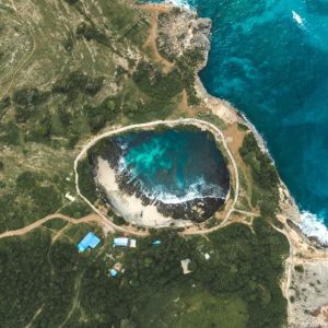
The Ultimate Guide to Angel’s Billabong of Nusa Penida
Nusa Penida, a purely immaculate island at the core of Indonesia, has morphed into a traveler’s paradise looking for solace away from the busy mainlands. Among the many...